Samsung's HBM Packaging Expansion Will Raise Demand for TSMC's CoWoS: How Taiwan and Korea Divide the Work in Advanced Packaging
During the week of November 9 to 13, 2026, everyone was watching the news of Nvidia CEO Jensen Huang stepping down. What may have been overlooked is that on November 12 and 13, four companies, Samsung Electronics, Samsung Electro-Mechanics, ASE and XinTec, together with TSMC, which signed an agreement with XinTec, announced major investments in HBM packaging and CoWoS advanced packaging. How these moves by leading chipmakers in Korea and Taiwan will affect the world is worth a close look.
Let's start with Korea. The Korean government announced that Samsung Electronics will invest 6 trillion won (about US$4.3 billion) to build a new plant dedicated to HBM packaging, and that Samsung Electro-Mechanics will invest 8 trillion won (about US$5.8 billion) to expand its production lines in Sejong for advanced packaging substrates for GPUs and CPUs. The government's support package covers permits, power supply, water supply and talent development, and groundbreaking ceremonies have been held for both projects.
Reading this news, many people will have a few questions. Is the Samsung group going to compete with TSMC's advanced packaging, CoWoS? Is the HBM packaging plant that Samsung Electronics is building for packaging HBM chips? Does it extend into the advanced packaging that puts HBM together with GPUs and other chips? Will this investment compete with TSMC's CoWoS?
The answer should be clear. Samsung's new plant packages "the HBM itself." It is not the advanced packaging that puts HBM and GPUs together. So it will not replace TSMC's CoWoS; if anything, it will increase demand for CoWoS.
Samsung's New Plant Packages the HBM Itself, and Finished HBM Still Has to Go Into TSMC's CoWoS
If you look closely at how an AI chip is packaged, it actually goes through two layers of packaging. The first layer is the packaging of the HBM itself, and the second is system-level 2.5D advanced packaging. The differences are as follows.
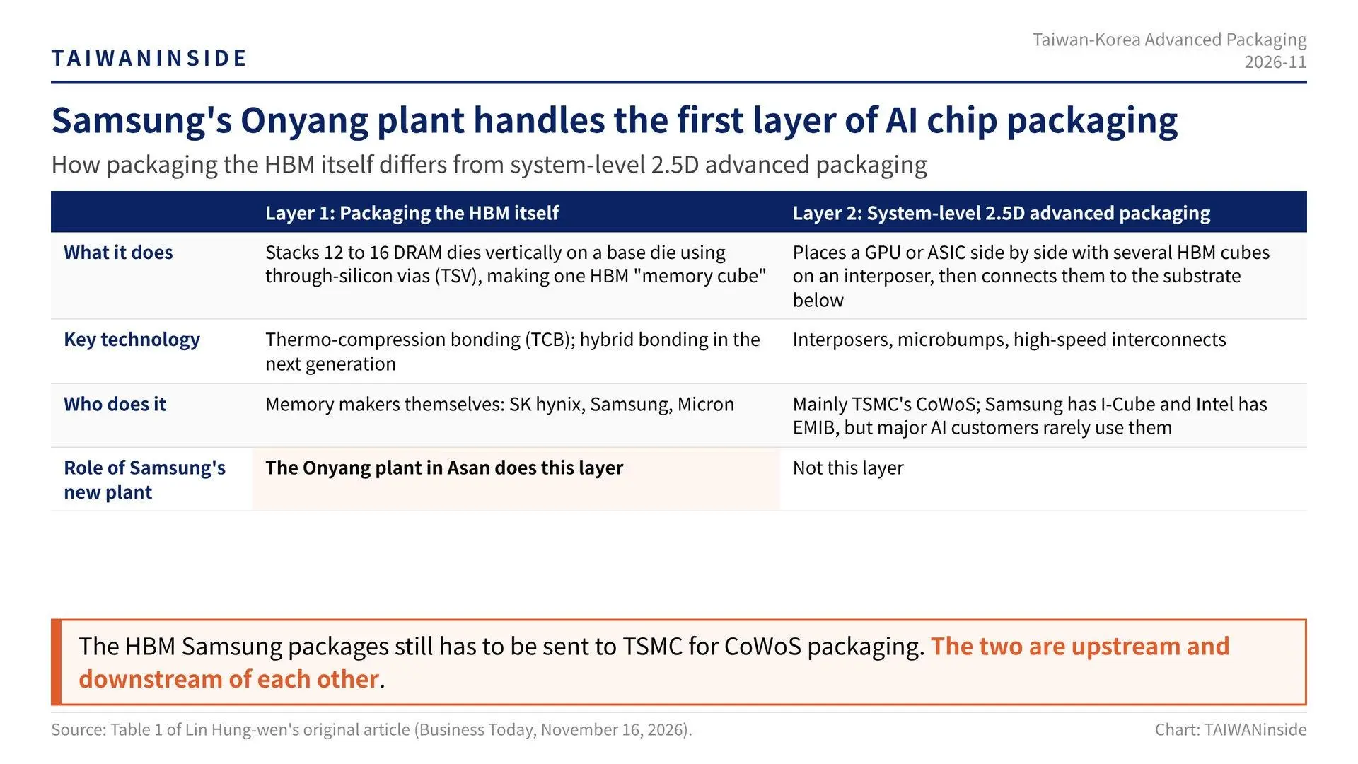
So the Onyang plant Samsung announced is mainly about the HBM stacking process. Today this uses thermo-compression bonding (TCB); the new plant will adopt hybrid bonding from the start, with equipment for volume production ready from day one. The goal is to produce next-generation HBM and catch up with SK hynix.
Let's look more closely at the difference between the two investments by Samsung Electronics and Samsung Electro-Mechanics.
For Samsung Electronics' HBM packaging plant in Onyang, Asan, the first phase is an investment of 6 trillion won for a three-story building with about 31,000 square meters of cleanroom. Another roughly 40 trillion won will then be spent on equipment, for a total of about 46 trillion won. Volume production was originally planned for 2029 and has now been brought forward a year, to June 2028. Samsung plans to link its Onyang and Cheonan sites to build a cluster for memory back-end processing.
As for Samsung Electro-Mechanics' substrate plant in Sejong, it plans to invest 8 trillion won by 2040, of which 4.3 trillion won goes to the new plant, with volume production in September 2028, making GPU and CPU package substrates for AI servers. The substrate is the bottom layer of a CoWoS package, so this investment also supplies the downstream end of CoWoS rather than competing with it.
So even with these two investments by the Samsung group, the world will still need TSMC's CoWoS in the future. It will not just need it; it will need even more of it.
That is because TSMC makes AI chips for Nvidia, AMD and Google, and the integration of HBM with GPUs, CPUs or TPUs is done almost entirely in TSMC's CoWoS. So the HBM that Samsung finishes packaging still has to be sent to TSMC for CoWoS packaging. The more HBM Samsung produces, the more HBM is sent to Taiwan for CoWoS packaging. The two are in an upstream and downstream relationship.
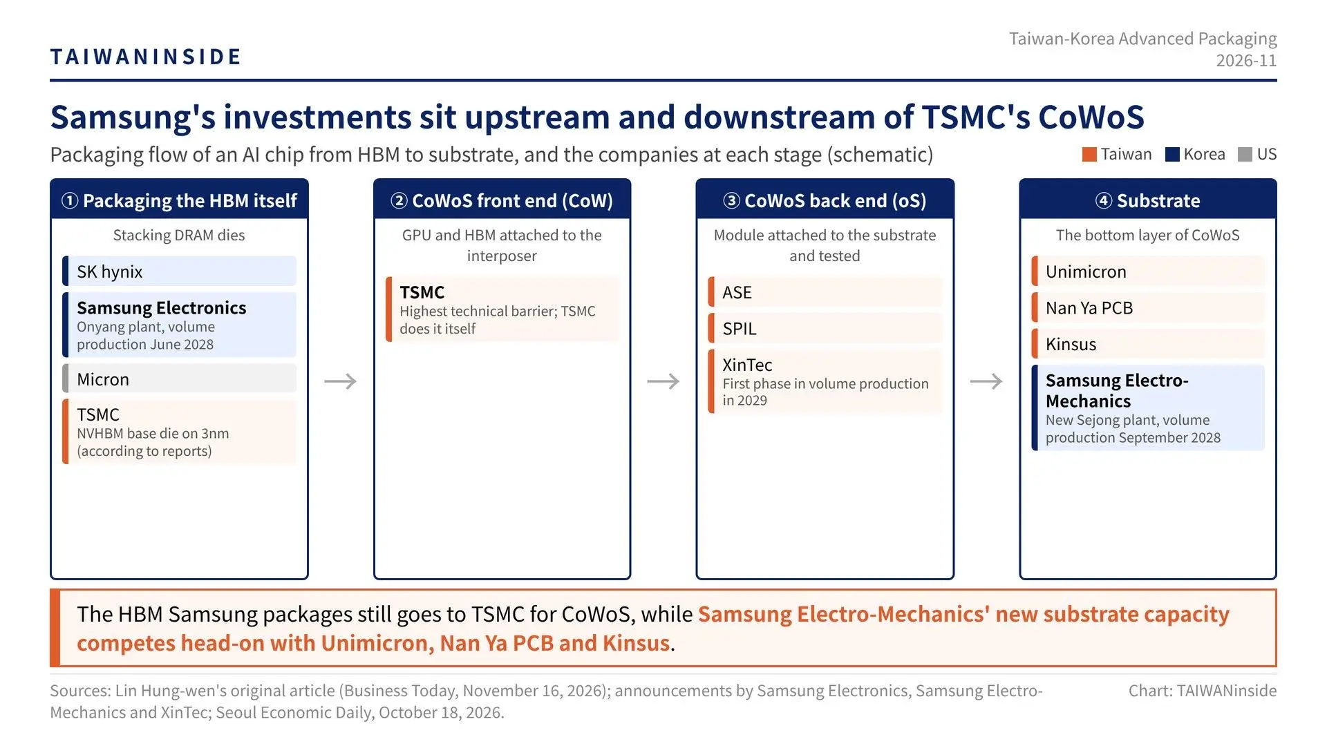
What's more, Samsung is even going to use TSMC to make part of its HBM. In October 2026, Nvidia asked the three memory makers to have the base die of its custom HBM (NVHBM, based on HBM4E) made on TSMC's 3nm process.
According to a report by Korea's Seoul Economic Daily on October 18, 2026, Samsung has already agreed, which means partly giving up its signature strategy of a one-stop "memory, foundry and packaging" package. The one-stop approach will remain only for standard HBM and other customers, such as AMD. In other words, the logic die at the very bottom of the HBM is moving from the memory makers to TSMC, and TSMC's role in HBM itself is actually growing.
As for Samsung's 2.5D packaging, it still has not broken into the mainstream. Samsung has I-Cube and has kept promoting its one-stop offering, but the advanced process technology of the major AI chip customers is all at TSMC, and Samsung's foundry division has received too few orders, so advanced packaging naturally stays at TSMC as well.
Samsung Electro-Mechanics Is Expanding AI Server Substrates, and the Pressure Falls on Taiwan's Substrate Makers
So when you look at the Samsung group's moves in HBM packaging, what really deserves attention is their impact on technology roadmaps in the short and long term.
In the short term, these two investments complement TSMC rather than threaten it. More HBM supply actually helps put CoWoS capacity to use. In the commentary accompanying its third-quarter results on November 17, 2026, Nvidia said its supply commitments rose from US$279 billion in the previous quarter to US$390 billion, mainly related to multi-year procurement of memory.
In the long term, the industry has long been studying how, once hybrid bonding matures, to stack HBM directly on top of logic chips (3D stacking). At that point, the division of labor between memory makers and foundries may be reshuffled. Samsung has memory, foundry and packaging all under one roof, so in theory it has the best chance of integrating them; but it must first prove that its advanced processes, such as 3nm and 2nm, can attract orders from major customers.
At this point, I should also point out that although Samsung's moves will not threaten TSMC, they may hit Taiwan's substrate makers. Samsung Electro-Mechanics' expansion of AI server substrates will compete head-on with Taiwanese substrate makers such as Unimicron, Nan Ya PCB and Kinsus. Once the capacity comes online in 2028, substrate prices and market share may both come under pressure.
In fact, Nvidia announced in October 2026 that within the next three years it will raise the substrate capacity its products need to 2.5 times the current level, and it reached capacity expansion plans with several supply chain partners. These partners include not only existing Taiwanese companies such as Unimicron, but also a new one, Korea's Samsung Electro-Mechanics. According to Korea's Maeil Business Newspaper, Nvidia and Tesla will together contribute about 3.7 trillion won to help Samsung Electro-Mechanics expand its substrate lines: about 2.6 trillion won from Nvidia for dedicated lines in Sejong and Busan, and about 1.1 trillion won from Tesla for the Sejong plant.
In other words, part of Samsung Electro-Mechanics' expansion was prepared for Nvidia from the start. What Taiwan's substrate makers face is sharing orders with Korean rivals inside Nvidia's supply chain.
Finally, there is one more angle worth discussing in the Korean government's announcement: how the Korean government helps its industry. Its support package this time covers permits, power supply, water supply and talent development. President Lee Jae-myung attended the groundbreaking ceremony in person, and construction can be finished a year earlier. Compare this with Taiwan's biggest bottlenecks today, power, water and talent. In the end, the AI race is a contest not only of companies' technology but also of whether a country can get factories built quickly.
TSMC Signs XinTec Through 2033 and Hands the Back End of CoWoS to Taiwanese Packaging Partners
In Taiwan, there were also two pieces of news on November 13, 2026. ASE opened the first phase of its Luzhu plant and broke ground on the second phase; with both phases at full capacity, total investment is estimated at NT$100 billion. XinTec also signed an agreement with TSMC running through the end of 2033 to set up back-end advanced packaging lines in TSMC's facility in the Central Taiwan Science Park, with the first phase planned for volume production in 2029, and approved the issuance of NT$15 billion in convertible bonds.
Put these two pieces of news together and they reveal the same thing: TSMC is handing the back-end process of CoWoS to its Taiwanese packaging and testing partners, forming an advanced packaging cluster that is "led by TSMC, with packaging and testing companies sharing the work." And XinTec, a company TSMC has invested in, signed an agreement running to 2033 right away, which shows that TSMC expects demand for advanced packaging to last at least another seven years.
First, here are the key points of these two pieces of news, in the table below:
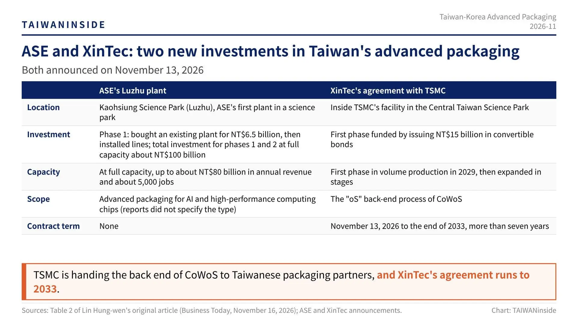
It is worth noting that XinTec's model of cooperation is unusual. CoWoS is roughly divided into two stages. The front end, "CoW," attaches the GPU and HBM to a silicon interposer. It has the highest technical barrier, and TSMC does it itself. The back end, "oS," attaches the whole module to the substrate below and then tests it, and its technical barrier is relatively lower.
XinTec's approach amounts to setting up its own production line inside TSMC's facility. XinTec pays for the equipment and the automated material handling system itself and is responsible for production and running the line, while TSMC provides the facility, packaging technology and manufacturing support.
This kind of cooperation benefits both sides. TSMC can concentrate its capital spending on the front-end CoW and the more advanced SoIC, and hand the lower-margin back end to XinTec, a company it has invested in. TSMC is XinTec's largest shareholder, with a stake of about 40%.
As for XinTec, a long-term agreement of more than seven years gives it visibility on revenue, which is why it dared to issue NT$15 billion in convertible bonds to expand capacity. After the news was announced, XinTec's share price jumped about 38% in a week, but on November 16, 2026, it fell by the daily limit, closing at NT$467.5.
Amid Concerns About an AI Bubble, Four Things the ASE and XinTec Investments Tell Us
So, looking at the investments by ASE and XinTec, there are at least four implications for Taiwan's advanced packaging industry.
First, Taiwan's advanced packaging has gone from "done by TSMC alone" to "shared across a whole cluster." In the past, CoWoS capacity was insufficient because TSMC could not expand fast enough on its own. Now TSMC does the hardest front end, while ASE, SPIL and XinTec take on the back end, so capacity can expand faster. Taiwan has gone from "having one very strong company" to "having a whole, very strong supply chain."
Second, a long-term agreement running to 2033 is a statement of confidence in AI demand. Many people are now discussing concerns about an AI bubble, yet TSMC is willing to sign with a partner through 2033, which shows it judges that demand for advanced packaging will last at least seven more years. Add the dual-chip packaging of Google's eighth-generation TPU and Samsung's HBM expansion, and the number of chips and HBM going into CoWoS will only keep rising.
This is one of the strongest pieces of industry evidence so far against the claim that "the AI bubble is about to burst." However, the agreement did not disclose its value, nor did it say whether it includes guaranteed purchase volumes, so how binding it really is remains to be seen.
Third, advanced packaging is forming two major clusters, in the south and in central Taiwan. In the south is ASE's Luzhu plant, linked to TSMC's advanced process and advanced packaging fabs in Kaohsiung and Chiayi. In central Taiwan, XinTec is moving into TSMC's Central Taiwan Science Park facility. Advanced packaging will spread from Hsinchu to central and southern Taiwan, driving local demand for equipment, materials and talent.
Fourth, compared with Korea, Taiwan's model of dividing the work is more flexible. Samsung follows a one-stop model of memory, foundry and packaging, but major customers are not buying it; even the base die of Nvidia's custom HBM has to go to TSMC. In Taiwan's model, TSMC holds the most critical technology and then shares capacity expansion with packaging and testing companies. Customers can get the most advanced process and packaging in one place, and Taiwan's packaging and testing companies benefit as a result.
Of course, investors also have things to watch. "oS" is a lower-barrier step in advanced packaging. Although it belongs to the core circle, its margins are lower than TSMC's CoW. Under the framework I have mentioned before, that "the closer to the chip, the more valuable," it sits on the outer edge of the core circle.
In addition, XinTec has to bear some risk. Because XinTec pays for the equipment itself, if demand falls short of expectations, the depreciation burden will fall on XinTec. If the convertible bonds are converted into shares, they will also dilute its share capital.
As for timing, ASE's Luzhu phase two and XinTec's first phase will not reach volume production until 2028 to 2029. What is being priced in now is long-term expectations, and the contribution to revenue in the short term is still limited.
Related Articles
Why TSMC Is Buying into Both OpenAI and Anthropic: Three Investment Principles from ASML and ARM to AI Model Companies
Come Up with a Way! How Former TSMC CTO Chenming Hu Extended the Life of Moore's Law and Showed TSMC How to Overtake Intel
Farewell to Jensen Huang: The Best Storyteller in AI Could Not Write His Own Ending. What Comes Next for Nvidia, the AI Industry and Taiwan's Supply Chain