No Accident: How Taiwan’s Small Equipment Makers Secured a Critical Role in TSMC’s AI Packaging Process While Global Giants Stayed Away
Hsinchu is the center of Taiwan’s semiconductor industry — and also the location of TSMC’s headquarters. In 1987, Morris Chang(張忠謀)founded the world’s first pure-play foundry here. Over the nearly four decades since, the world’s most advanced semiconductor process technologies have been exported from this city.
Every year at this event, TSMC publicly honors the suppliers that made the biggest contributions that year. The list of winners circulates openly within the industry, effectively serving as TSMC’s endorsement of those companies. Applied Materials, KLA, Tokyo Electron(TEL), Lam Research, Shin-Etsu Chemical, Merck and others are regular names on the list.
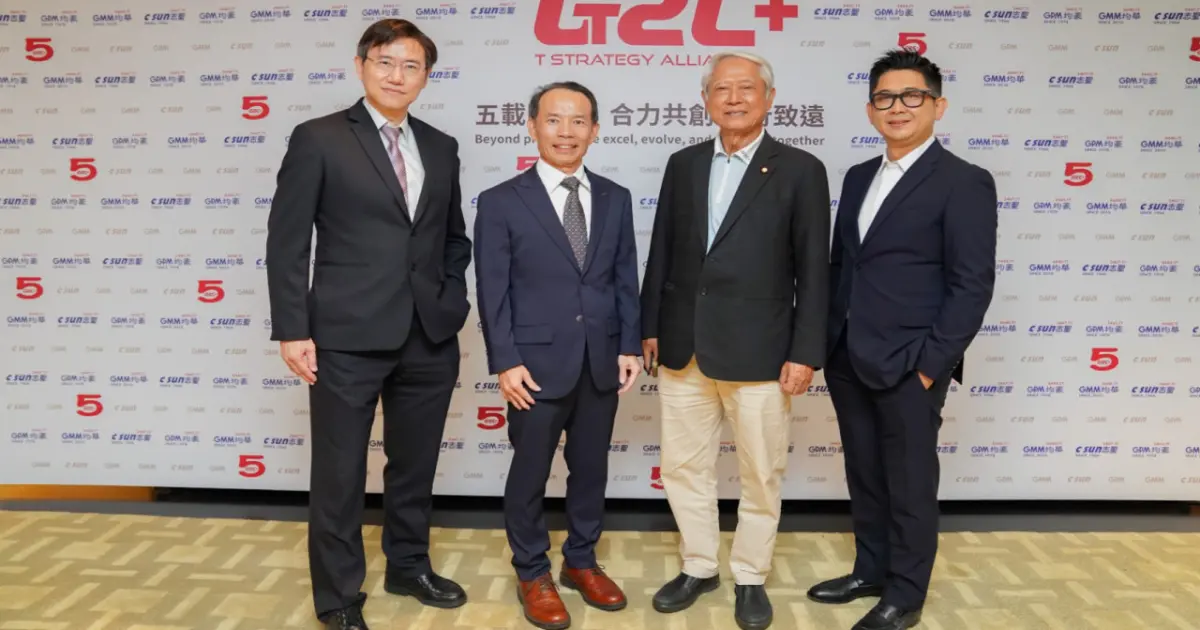
Liang Yu-wen(梁又文), CEO of CSUN(志聖工業), remembers that for as long as 10 years, his company could only wait outside. Around 2019 and 2020, CSUN finally got a chance to enter the room, with its seats placed in the very last row. “Over the past two years, we finally managed to move forward — and even go on stage to receive awards,” Liang said with a laugh.
CSUN and GMM(均華精密)were able to squeeze into TSMC’s supply-chain ecosystem entirely because the explosive demand for AI training chips drove a rapid expansion in CoWoS advanced-packaging capacity.
NVIDIA’s high-end general-purpose AI chips — including the H100, H200 and B200 — all require TSMC’s CoWoS advanced-packaging technology to package GPUs together with high-bandwidth memory(HBM). CSUN’s lamination and baking equipment, GMM’s die bonders and GPM’s(均豪精密)automated optical inspection(AOI)equipment are all part of that process.
The Four Young Dragons of CoWoS Packaging
The G2C+ Alliance, led by CSUN CEO Liang Yu-wen, consists of four Taiwanese small and midsize equipment makers: CSUN(志聖工業), which provides lamination and thermal process equipment; GPM(均豪精密), which provides grinding and inspection equipment; GMM(均華精密), which provides die bonders and die sorters; and CONTREL(東捷科技), which provides laser cutting and glass-substrate processing.
Together, these four companies cover multiple critical process stations in TSMC’s CoWoS advanced packaging. Members of the G2C+ Alliance are key players in the vast and complex ecosystem behind AI chips.
Over the past five years, the alliance’s combined market value in Taiwan’s stock market has increased tenfold to $4.8 billion. In the first quarter of 2026, CSUN reported earnings per share of NT$3.06, up 209% year on year, while GMM reported EPS of NT$5.19, up 220%.
But Liang said the growth is still only at its starting point. Last year, CSUN and GMM each generated about NT$1.5 billion in semiconductor revenue, accounting for only about 1.5% of TSMC’s advanced-packaging capital expenditure. TSMC’s total annual capital expenditure reached $56 billion, while G2C+ accounted for less than 0.1% of that amount.
As TSMC massively expands advanced packaging, how much can that 0.1% grow? And what is the next step in the evolution of CoWoS technology? These are the questions this article seeks to answer.
CoWoS: The Essential Foundation of AI Chips
CoWoS is an advanced-packaging technology TSMC began developing in 2009. Its full name is Chip-on-Wafer-on-Substrate.
The method places multiple chips horizontally and packages them on the same silicon interposer, shortening the signal-transmission distance between the GPU and high-bandwidth memory(HBM)to an extreme degree. Compared with conventional packaging, bandwidth increases severalfold, latency drops sharply and power consumption falls at the same time.
After TSMC developed the technology, it remained quiet for nearly a decade.
When ChatGPT emerged in 2022, AI model parameter counts jumped from the tens of billions toward the trillion scale. The computing bottleneck shifted from transistor density inside chips to data-transfer bandwidth between chips. A GPU can perform trillions of operations per second, but if memory cannot feed data quickly enough, the GPU can only wait. Conventional packaging places the GPU and memory separately on a circuit board, with copper wires connecting the two. The signal has to travel a long distance, with narrow bandwidth and high latency. CoWoS packages the two on the same silicon interposer, shrinking the distance from centimeters to micrometers, increasing bandwidth severalfold and reducing power consumption at the same time.
As a result, CoWoS became standard equipment for high-end AI training chips almost overnight.
CoWoS is a proprietary advanced-packaging technology led and developed by TSMC. It integrates “wafer manufacturing” and “packaging” into the same process flow, with TSMC controlling yield throughout the entire process. But CoWoS actually consists of two different process stages, with different degrees of control.
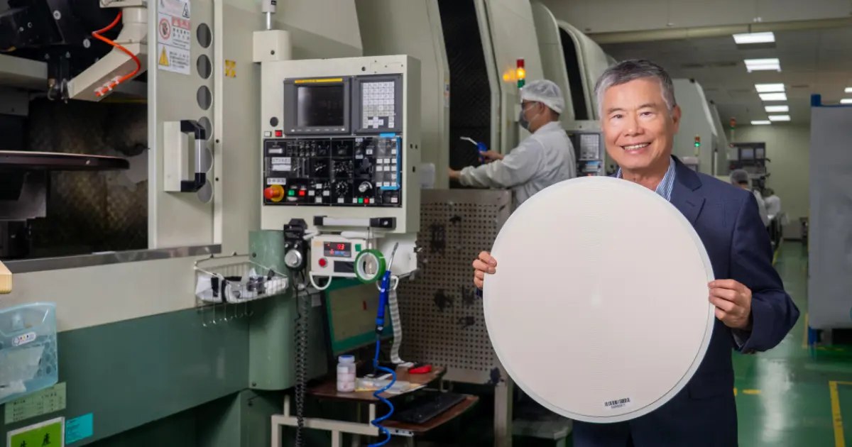
The first stage is called CoW(Chip on Wafer). Inside the cleanroom of a wafer fab, TSMC fabricates the silicon interposer, then precisely bonds the GPU chip and HBM memory onto the interposer using through-silicon via(TSV)technology. This stage requires wafer-fab-level equipment and precision. It is a core technology for TSMC, and traditional packaging and testing providers have difficulty entering it. CSUN’s lamination and baking equipment and GMM’s die bonders are deployed in this part of the process.
The second stage is called oS(on Substrate). It cuts the completed CoW assembly, packages it onto a substrate and then performs testing. This stage has a relatively lower technical threshold, and TSMC outsourced it early on to traditional packaging houses such as ASE(日月光)and SPIL(矽品).
According to TSMC’s data, monthly CoWoS capacity rose from about 13,000 wafers in 2023 to about 37,000 in 2024, then reached 70,000 in 2025. By the end of 2026, the target is to exceed 110,000 wafers per month, representing three consecutive years of substantial doubling-level growth.
Yet demand growth for AI chips is more than twice the speed of TSMC’s CoWoS capacity expansion. TSMC Chairman C.C. Wei(魏哲家)said on a 2024 earnings call: “Capacity will double in both 2025 and 2026, but it still will not meet demand.”
Holding Out for 14 Years: Why Taiwan’s Small Companies, Not Global Giants?
Premium Members Only
This is a premium article. Please join our membership to read the full content.
Become a member to unlock all in-depth reports and exclusive analysis.
Already a member? Login Now
Related Articles
From a Single Lawyer’s Letter to a NT$26.4 Billion Market Cap: The Story Behind PVI’s 67% Gross Margin

The Wealth of a Tech Island: Decoding Taiwan's "Thousand-Dollar" Stock Surge and One Veteran Investor's $300M Masterclass
The Silicon Valley Playbook for "AI Defense" is Here: Why Taiwan's Digital Defense Gap is the Next Big Opportunity for Global Tech